
Arranging footprints
Align, distribute, arrays and the Arrange flyout.
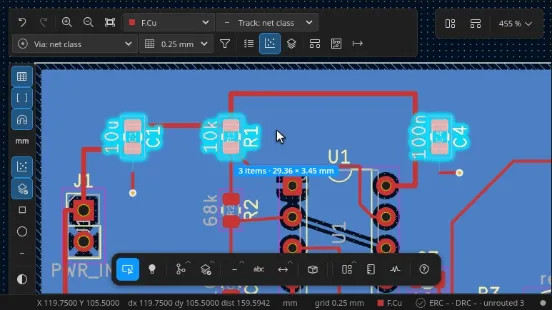
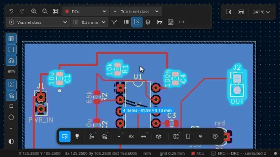
The board tool bar’s Arrange flyout works on the selection: Align left / right / top / bottom / centre X /
centre Y (to the extent of the selection), Distribute horizontally or vertically (equal gaps, or equal centre
spacing; the two outer items stay), Create array… (Ctrl+T: copies on a grid of columns × rows with a pitch,
or on a circle with a count, centre and angle, optionally rotated, each copy renumbered after the highest reference
of its prefix), Swap positions (S, two items exchange places, footprints also rotation and side), Flip
to back, Group / Ungroup and Lock / Unlock. A click on a member of a group selects the whole group;
Alt+click selects the single item. The same edits are the commands pcb.align, pcb.distribute, pcb.array,
pcb.group, pcb.ungroup, pcb.lock, pcb.swap and pcb.flipToBack (edsnx pcb align board.kicad_pcb --ids … --mode left).
Pack footprints (P, KiCad’s Pack and Move Footprints) packs the selected footprints into a compact block at the top-left of the selection, largest first, 1 mm apart; move the block afterwards with M. The whole pack is one undo step (clip).
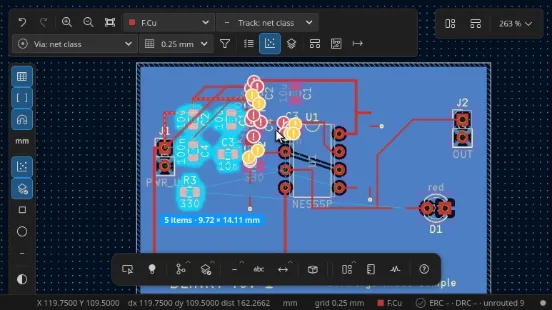
Locked items stay where they are in every placement tool: Align uses the locked items of the selection as the line the others align to (clip), Distribute leaves them out (clip), Create array does not copy them (clip) and Pack packs only the unlocked footprints. The status bar says how many were left in place. Each of these tools shows its tool card (see Tool cards).
Moving footprints with their copper#
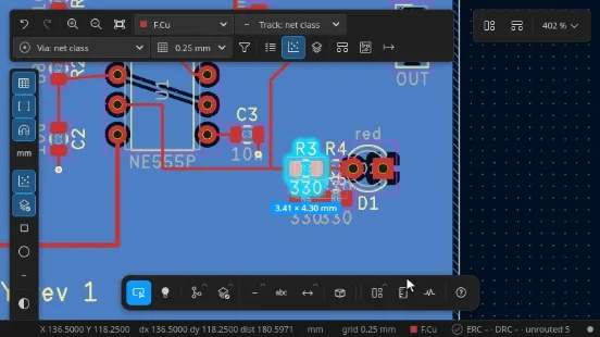
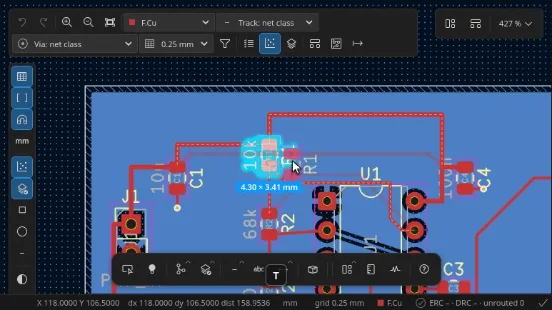
When a footprint moves (M, a drag, R to rotate, F to flip while moving), its tracks come along. The
tracks that leave each pad are its attached copper: the run of segments from the pad to the next pad, via,
junction or open end. How they adapt is the attached-copper mode. Choose it in Routing ▸ Drag ▸ Footprint
tracks or in the Placement panel (Moving footprints ▸ Tracks), or press T while moving to cycle through
the modes (clip). The choice is remembered as
softforge.edsnx.move.attachedCopper.
| Mode | While moving | On the drop |
|---|---|---|
| Rubber band (default) | The run stretches from the moved pad and re-corners at 45° to where it ran before; the tail stays. | The stretched tracks. |
| Re-route | The run is drawn as a dashed ghost. | The run is ripped and routed again, from the pad to its fixed end, with the walkaround router (clearances of the net classes). If no route is found, the run is stretched instead and the status says so. |
| Rip up | The run is shown as a ratsnest line. | The run is deleted; the ratsnest shows the connection. |
| Keep | Nothing changes. | The tracks stay where they were. |
- Rotate and flip. The runs follow the rotated pads. A flip moves SMD pads to the other side. Each run then keeps its layer up to a new via next to the pad, and a short track on the new side reaches the pad. The via takes the size of the net class and keeps hole-to-hole distances. If the run already ends on a through via that carries a track on another layer, the whole run moves to the pad’s new side and ends on that via, with no new via. If no via fits, the run is ripped up and the move reports it.
- Groups. Tracks and vias between the selected footprints move rigidly with them. Only the runs that leave the selection adapt.
- Vias in pads move with the pad. Their tracks on the other layers adapt like runs from the pad.
- Push components (Routing ▸ Drag or Placement ▸ Push components,
softforge.edsnx.move.componentShove): footprints whose courtyards the moving part overlaps are pushed aside along the move, in a chain if needed. They spring back when the part moves on. The pushes stop at locked parts, at the board edge and after a limit of pushes. In those cases nothing is pushed and the overlap is reported. - Live placement checks (Placement ▸ Live placement checks,
softforge.edsnx.move.placementChecks, on by default): while moving, the live-check markers show courtyard overlaps, holes inside another courtyard, hole-to-hole and hole clearance, copper clearance (the adapted tracks included), the board edge, keepouts and silkscreen over pads. A pour that the move would split, a pad that would lose its pour connection, and a thermal spoke the move would cut are reported as warnings. The status bar counts the errors and warnings, and the drop is never blocked. - Snapping. With item snapping on, the moving part snaps to the courtyard edges of the parts around it and lines its pads up with their pad rows and columns. Blue guide lines show the alignment.
The whole move is one undo step: the footprints, the adapted tracks, the new vias and any pushed parts. Agents and
scripts use the command pcb.moveFootprint:
edsnx pcb move-footprint board.kicad_pcb --refs U3 --by 5,0 --tracks reroute
edsnx pcb move-footprint board.kicad_pcb --refs C4 --flip --checks strict    # refuse a move with placement issues
--tracks takes the mode (rubberBand, reroute, ripUp, keep). --shove pushes overlapped parts.
--checks is warn (the default: apply the move and list the issues), strict (refuse a move with issues)
or off. The result lists the issues, what happened to each run, and the parts that were pushed.